well a lot of you must have heard of the term fpga and with some digging and youtube videos u get a picture that it is basically a minecraft equivalent for hardware engineers
with an fpga you can think of any digital ckt that does a certain functionality describe the circuit in something called a HDL (hardware description language) dump the code on the fpga and voila the fpga builds the ckt in real time and let’s u play around with it the best part being u can erase your existing design and dump some new hdl to simulate another digital ckt
why should you care??
The latest fpga’s can boot linux on a cpu core that is completely written by you from scratch how cool is that !!!!
well that’s the basic gist of what an fpga is but let’s dive deep into how an fpga is built and how this magic has come to be
ARCHITECTURE Link to heading
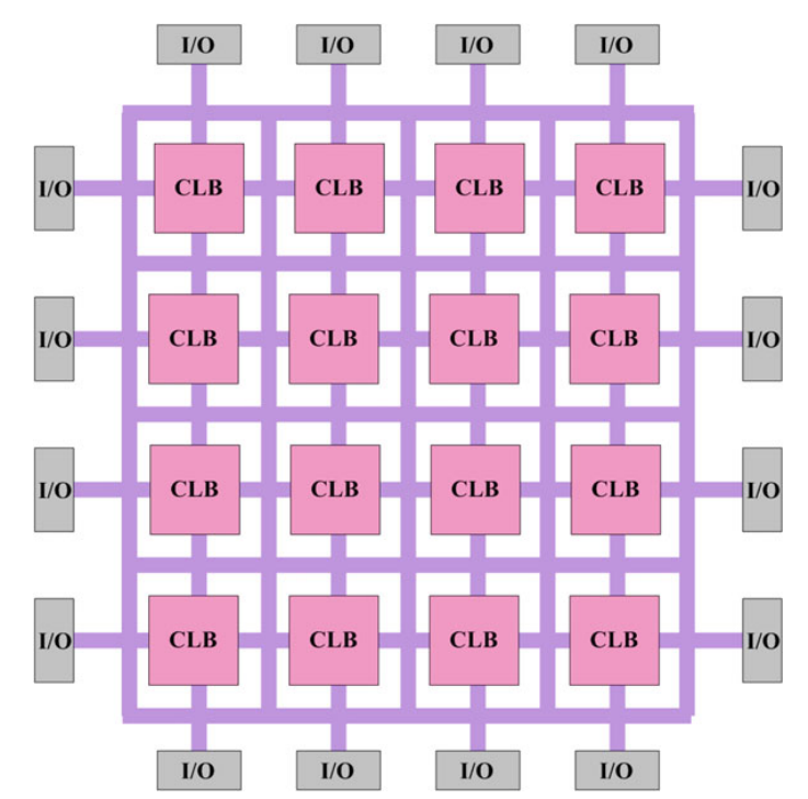
so the complete brief architecture can be divided into 3 major blocks and don’t stress abt the terminologies we’ll go thru it as we progress
configurable logic block (CLB)
interconnect fabric that connects these (CLB)
(interconnect fabric= fancy name for programmable wires that connect the CLB’s)
i/o blocks that are connected to CLB’S thru interconnect fabric
CLB (configurable logic block) Link to heading
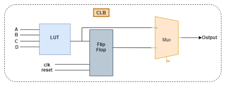
the above picture descirbes what a clb basically is it’s a connection of an lut a mux and a flip flop we need a flip flop in CLB to implement sequential logic and another mux to select b/w the combinational and sequential o/p
but what’s an LUT?? Link to heading
it’s nothing but a 1 bit wide ram that is read by a mux to implement any digital logic the below example will give u a clear idea
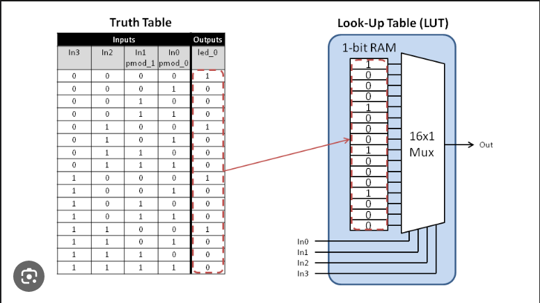
so the truth table has 16 o/ps that is mapped to an sram and now we need a multiplexer with 4 ips to implement the boolean function
INTERCONNECT FABRIC Link to heading
now here is where the magic happens and the complexity arises there are various design constraints in connecting these CLB’S and various proposed architectures in solving them in this blog I’ll be discussing the island style routing architecture
As discussed earlier, in an FPGA, the computing functionality is provided by its programmable logic blocks and these blocks connect to each other through a programmable routing network called the interconnect fabric.
The routing interconnect of an FPGA consists of wires and programmable switches that form the required connection. These programmable switches are configured using the programmable technology
ISLAND STYLE ROUTING ARCHITECTURE Link to heading
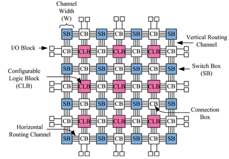
in this architecture the FPGA routing network consists of horizontal and vertical routing tracks which are interconnected through switch boxes (SB). Logic blocks are connected to the routing network through connection boxes (CB)
CONNECTION BOX Link to heading
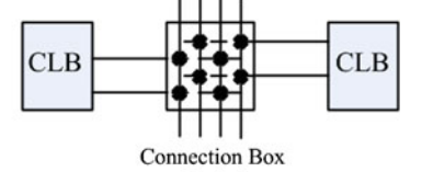
well a connection box is basically a block that connects the CLB to the routing network
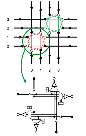
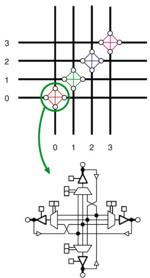
SWITCH BOX Link to heading
a switch box is used to connect the vertical and horizontal routing tracks
now there are 2 types of switch boxes uni directional and bi directional
uni directional allows signal to flow in one direction
bi directional allows signals to flow in both the directions
the figures for both are given below
- uni directional
- bi directional
I/O BLOCKS Link to heading
i/o ports in an fpga are of various kind and have a lot of customization options
modern fpga’s have slots for vga,audio/video sd card and many more some differentiating properties of fpga i/o blocks are below
Highly Configurable pins for input, output, or bidirectional signals.
Adjustable parameters like voltage levels, slew rate at ip and op ports.
Offers differential signaling, high-speed transceivers, ADCs, DACs, etc.
Organizes I/O blocks into banks for better signal management.
there are also dedicated custom PLL blocks for custom clock signals generation
so yea with this the blog ends thou this is a very rudimentary picture of the internals of an fpga and there is so much more the purpose of the blog was to give u guys a peek into the exciting world of how fpga’s works.
thanks for sticking thru and would love to hear from you regarding any feedback or queries
ad`ios..